Expansions: Henkel breaks ground on EUR120 mn adhesives facility in China; Wacker to expand semiconductor grade polysilicon capacity in Germany
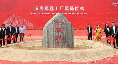
Industrial firm Henkel recently broke ground on a new manufacturing facility of its Adhesive Technologies business unit within the Yantai Chemical Industry Park in Shandong Province, China. With an investment of approximately EUR120 million, the new plant, titled with the Chinese name ‘Kunpeng, will enhance Henkel's production capacity of high-impact adhesive products in China, and further optimise the supply network, to better meet the growing demand from domestic and international markets.
The Kunpeng plant is set to occupy more than 150,000 sq m, including state-of-the-art automated production workshops and an 8,000 sq m smart warehouse. The new plant will enhance Henkel's supply capacity of high-impact adhesive products in the Chinese market. The plant aims to fully meet the demand of fast-growing industries including electronics, automotive, medical, equipment manufacturing, and aerospace, with high-quality and sustainable adhesive products and solutions.
Mark Dorn, Henkel Executive Vice President of Adhesive Technologies, highlighted the significance of the new plant: “China plays an important role in our operations at Henkel and continues to demonstrate economic resilience and growth. Investing in the Kunpeng plant reflects our strong commitment to the future of our business in China and the Asia-Pacific region, creating value for our customers.”
“Kunpeng, our state-of-the-art facility, will set a new industry standard with its modernization and sustainability design, keeping us ahead of the curve and meeting evolving customer needs,” says Rajat Agarwal, President of Henkel Greater China. “China’s focus on achieving high-quality and sustainable development creates unique opportunities for technology and product advancements. Investing in Kunpeng enables us to provide unparalleled support to our customers with enhanced end-to-end capability.”
The plant will utilise 100% renewable electricity and incorporate a range of sustainability features such as an advanced building energy management system, water circulation system, and a ground source heating pump system. These technologies are expected to reduce carbon dioxide emissions by more than 5,000 tonnes/year and reduce operational water consumption by 25%, contributing to Henkel's ambition of achieving climate-positive operations in its manufacturing by 2030.
In other news, Munich-based Wacker Chemie AG announced its intention to expand its capacity for cleaning semiconductor-grade polysilicon. Accordingly, there are plans to set up a new production line at the company’s Burghausen site by early 2025. The new plant will increase existing capacity at the site by well over 50%. The etching of polysilicon chips is the crucial step in production to ensure the material surface purity required for semiconductor applications. Capital expenditures for the project are expected to exceed EUR300 million. This will create not only more than 100 new jobs at Wacker’s Burghausen site but also additional jobs at partner companies.
As well as expanding capacity, the project includes substantial capital expenditures for research and innovation. The aim here is to further increase the purity of polysilicon by means of new, highly automated processes, thus enabling semiconductors to meet even smaller design rules and making chips even more powerful.
Wacker applied for funding for this part of the overall project under the EU’s Important Projects of Common European Interest (IPCEI) program. In this regard, the European Commission granted the necessary approval under state aid law on June 8, 2023. If the application is now approved by the German Ministry of Economic Affairs and Climate Protection, Wacker expects to receive funding of up to EUR46 million.
“As the only European producer of ultrapure polysilicon, we are proud to be making an important contribution to strengthening Europe’s microelectronics supply chain with this project,” explained Wacker CEO Christian Hartel. He went on to say that, at the same time, this investment project was an important part of Wacker’s strategy to intensify its focus on polysilicon for applications that demand extremely high quality.
“By expanding our surface-cleaning capacity, we are creating the necessary conditions for meeting the continued fast-growing demand of our semiconductor customers. Thanks to this investment, we are also able to take the quality of our material to the next level so as to support the semiconductor sector’s latest technologies,” he added.
When the company introduced its new growth targets in March of last year, it announced that, in addition to producing material for solar cells with a particularly high efficiency, it would, going forward, expand its polysilicon capacity for semiconductor applications.
Wacker plans to double its sales with semiconductor-sector customers by 2030. It has earmarked investment of some EUR100 million for each of the next few years.
Cleaning the surface of the polysilicon chunks used as a starting material for making semiconductor wafers is a complex and technically very demanding process. Strong acids are used in an etching process to remove the uppermost layer from the surface of the polysilicon. The polysilicon is then packaged under cleanroom conditions for shipment to customers. The use of state-of-the-art technologies and a high degree of automation means that the new facilities achieve a surface purity that already meets the ever-greater demands required for future generations of semiconductor wafers.
(PRA)
Subscribe to Get the Latest Updates from PRA Please click here
©2023 Plastics and Rubber Asia. All rights reserved.

©2023 Plastics and Rubber Asia. All rights reserved.
Home Terms & Conditions Privacy Policy Webmail Site Map About Us