
2016-2017 Exhibitions
Carbon Nanotubes: Advancing industry with the power of small
Also, download this story from the electronic issue here
With carbon nanotubes (CNTs), the market is closer to having an environmentalfriendly nanomaterial that possesses ideal properties – superior strength, speed, flexibility, lightweight and thinness – all rolled into one, in this report.
Super material captured from carbon emissions
Greenhouse gas emissions have been going up and are projected to spiral to 500 parts per million (ppm) at the end of this century. It is for this reason that scientists are looking at ways of reusing the massive amounts of CO2 to produce carbon nanotubes (CNTs), which are tiny tubes consisting of rolled up sheets of graphene, 10,000 times thinner than a human hair, 100 times stronger than steel but only one-sixth as heavy.
In 2009, a research team from George Washington University (GWU), led by Chemistry Professor Stuart Licht, introduced a solar process that can convert atmospheric CO2 into highly valued carbon nanofibres. The solar thermal electrochemical process (STEP) makes use of the full spectrum of sunlight and thus captures more solar energy than the most efficient solar cell or photoelectrochemical processes, the group said.
This breakthrough is now being eyed for application to CO2 emissions of power plants, according to the GWU researchers who initially focused the study on the combined cycle (CC) natural gas power plants, which are the most efficient kind of electrical power plant yet still emit massive amounts of CO2.
The process can be undertaken by adding a molten lithium carbonate electrolyser to a conventional CC plant, creating a CC carbon nanofibre (CC CNF) plant. Using electrolysis, CO2 is split into oxygen gas and solid CNFs; and adding in small quantities of nickel, causes CNFs to be hollow, forming CNTs.
To make sure that it is feasible, in a new study, the same researchers performed a thermodynamic assessment of the proposed CC CNF plant. They found that the concept is economically feasible and even improves the power plants' energy efficiency. Using the new method, the researchers also estimate that it would cost just US$2,000/tonne to produce CNTs, which is less than 1% of current production costs. In view of this, the researchers are working to build and implement the technology rapidly.
High-valued commodity
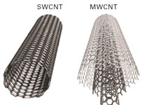
CNTs are normally categorised as either singlewall nanotubes (SWNT), with a diameter of about a nanometre; or multi-wall nanotubes (MWNT), with diameter ranging from 5 to 50 nanometres.
The basic materials used to produce CNTs are iron, cobalt, hydrogen, ceramic catalysts and gases such as methane and acetylene hydrogen.
CNT’s increasing adoption in end-use industries including polymers, electronics, energy, marine, aerospace and automotive, is driving its growth projected to reach an average of US$3.4 billion by 2022, as forecast by Grandview Research, projecting consumption to exceed 20,000 tonnes through the forecast period.
By 2024, the CNT market is anticipated to balloon past US$ 8.1 billion, according to latest research report by Global Market Insights.
CNT market is including, but not limited to, structural and conductive polymer composites, conductive adhesives, fire retardant plastics, metal matrix composites, Li-Ion batteries. SWCNTs and MWCNTs serve end user industries, such as aerospace & defence, energy, sporting goods, automotive, industrial, and electrical & electronics, and others.
Growth market regions are led by Asia Pacific as the largest, accounting for more than 40% of global volume in 2014, Grandview Research says. It adds that China and India are prime movers, with their growing plastic and composite industries coupled with domestic demand and comparatively low manufacturing cost than in other matured regions. Moreover, the healthy performance of the electronics sector in China, South Korea, Singapore, Taiwan and Japan will also make a positive mark on the CNT market in the coming years.
Along the same vein, research specialist, Technavio, predicts that Asia’s prime lead in the embedded systems markets could bode well for CNT growth. It adds that the region represents 66% of the microelectromechanical systems (MEMS) technology in electronic products, an emerging application for CNTs.
Ace material for flexible electronics
Applications are diverse as CNTs prove to have more edge than popularly used materials like silicon and films like Indium tin oxide-(ITO) coated films used in touch screens, LCD displays, solar cells, organic light emitting diode (OLED), and other electronic displays.
The potential of CNT as a viable material option for ITO-based films in flexible wearable electronics is what Japanese scientists from the National Institute of Advanced Industrial Science and Technology are developing, such as body sensors that could provide continuous monitoring of a person's blood pressure.
The researchers reviewed the latest use of CNTs in manufacturing as an important component of optoelectronic devices called transparent conductive films (TCFs). The latter are thin films of a material that is optically transparent and electrically conductive and a key component of everyday gizmos: smartphones, tablets, laptops, and flat screens as well as solar cells. The market for TCFs is expected to reach US$1.2 billion by 2025.
Currently, electronic gadgets are manufactured using ITOs, which has excellent electrical conductive properties but poor flexibility, making it unsuitable for wearable devices. Plus, it is also expensive to source and process.
CNTs, which exhibit high theoretical electrical conductivity, are an appealing alternative, cost-wise, due to their commercialisation for applications such as water filtration systems, sports equipment, and batteries and conductors. Prices could be lowered further by improving manufacturing processes, according to researchers Ying Zhou and Reiko Azumi.
“Sensing devices, such as wearable touch panels, are the most promising application for CNT-based TCFs. Two companies in Japan are already using CNTs to manufacture touch panels for mobile electronics,” the researchers said. They explained that OLEDs, which are already used to manufacture thinner, lighter and more efficient TV screens, are another promising application for CNT-based TCFs. But other materials used in their manufacture, such as metal nanowires, have higher conductivity and transparency and thus result in a better performance.
“Based on the overview of the fabrication, properties and possible applications of CNT-based TCFs, it can be concluded that current CNT-based TCFs still do not meet the demands of performance/cost for industrial use,” the researchers wrote in their review published in the Science and Technology of Advanced Materials journal. Manufacturing costs need to be reduced while their conductivity and transparency need to be improved, they said, recommending further enhancement of CNTbased TCFs.
Outshining silicon in transistor applications
But there is one area where CNTs have been proven. According to University of Wisconsin-Madison engineers, CNT transistors outperform silicon transistors, achieving a current that is 1.9 times higher.
The team, led by Michael Arnold and Padma Gopalan, UW–Madison Professors of Materials Science and Engineering, says that this breakthrough in performance is advancement towards exploiting CNTs in logic, high-speed communications, and other semiconductor electronics technologies. Moreover, it could usher the replacement of silicon transistors for the computer industry. “The new transistors are particularly promising for wireless communications technologies that require a lot of current flowing across a relatively small area,” Arnold adds.
CNT transistors should be able to perform five times faster or use five times less energy than silicon transistors, according to extrapolations from single nanotube measurements. The nanotube’s ultra-small dimension makes it possible to rapidly change a current signal traveling across it, which could lead to substantial gains in the bandwidth of wireless communications devices.

The UW–Madison team used polymers to selectively sort out the semiconducting nanotubes, achieving a solution of ultra-highpurity semiconducting CNTs, and thus solving the challenge of isolating purely CNTs (because metallic nanotube impurities act like copper wires and disrupt their semiconducting properties)
“We have identified specific conditions in which you can get rid of nearly all metallic nanotubes, where we have less than 0.01 % metallic nanotubes,” says Arnold.
The team also surmounted the challenge of nanotube alignment, with just the right spacing, when assembled on a wafer. Thus, the researchers developed a technique, called “floating evaporative self-assembly,” that gives them placement and alignment control of the nanotubes.
The nanotubes must make good electrical contacts with the metal electrodes of the transistor. Because the polymer the UW–Madison researchers use to isolate the semiconducting nanotubes also acts like an insulating layer between the nanotubes and the electrodes, the team “baked” the nanotube arrays in a vacuum oven to remove the insulating layer, resulting in excellent electrical contacts to the nanotubes.
The researchers also developed a treatment that removes residues from the nanotubes after they’re processed in solution.
The team is also working on adapting their device to match the geometry used in silicon transistors, “which get smaller with each new generation”. Moreover, they are also developing high-performance radio frequency amplifiers that may be able to boost a cell phone signal. While the researchers have already scaled their alignment and deposition process to 1 in. x 1 in. wafers, they are working on scaling the process up for commercial production.
Strengthening composite polymers for aerospace use
Meanwhile, the largest application segment for CNT is polymers, accounting for over 60% of global CNT market volume in 2014, according to Grandview Research. CNT as a filler reinforces polymers in composites for better electrical, thermal and mechanical strength of the end product. Armed with improved properties for heavy duty performance but much lighter weight, composites reinforced with CNTs find ideal applications in the aerospace sector.
But composite materials are also surprisingly vulnerable. While aluminium can withstand relatively large impacts before cracking, the many layers in composites can break apart due to relatively small impacts. Now, Massachusetts Institute of Technology (MIT) aerospace engineers have found a way to bond composite layers in such a way that the resulting material is substantially stronger and more resistant to damage than other advanced composites.
MIT engineers fastened the layers of composite materials together using CNTs. They embedded tiny “forests” of CNTs within a glue-like polymer matrix, then pressed the matrix between layers of carbon fibre composites. The nanotubes, resembling tiny, vertically-aligned stitches, worked themselves within the crevices of each composite layer, serving as a scaffold to hold the layers together.
In experiments to test the material’s strength, the team found that compared with existing composite materials the stitched composites were 30% stronger, withstanding greater forces before breaking apart.

This work was supported by Airbus Group, Boeing, Embraer, Lockheed Martin, Saab AB, Spirit AeroSystems Inc., Textron Systems, ANSYS, Hexcel, and TohoTenax through MIT's Nano-Engineered Composite aerospace STructures (NECST) Consortium and, in part, by the US Army.
Though further work needs to be done, MIT says the improvement may lead to stronger, lighter airplane parts, particularly those that require nails or bolts that can crack conventional composites, generating savings in fuel and costs.
(PRA)


Copyright (c) 2016 www.plasticsandrubberasia.com. All rights reserved.