Expansions: LG Chem expands CNT capacity with new unit; Merck’s EUR20 million investment for electronic materials in Japan
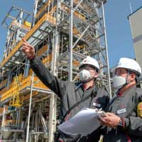
South Korea’s LG Chem has completed its 1,200-tonne expansion of the Yeosu CNT Plant 2 in what it says is the largest Carbon Nanotube (CNT) plant in the country. The company is robustly targeting the rapidly growing CNT market, widely used as the material for cathodes in electric vehicle batteries. Combined with the existing 500 tonnes, LG Chem has obtained a total capacity of 1,700 tonnes.
CNT is a new-generation material with the same level of electrical and thermal conductivity as copper and diamond, and 100 times the strength of steel. Due to its excellent properties that surpass existing materials, CNT has an infinite range of applications in batteries, semiconductors, automotive components, and surface heating elements.
LG Chem’s new CNT Plant 2 was constructed as the world’s largest single-line production facility with a self-developed fluidised bed reactor. The plant has achieved stable quality control and process innovation through complete automation that has reduced power consumption by 30%.
The CNT produced at this plant will be supplied to battery companies such as LG Energy Solution as a conductive additive. Its applications will be extended to a wide range of industries. As the CNT market continues to grow, LG Chem plans to launch the third plant this year and continue expanding its capacity in the future.
LG Chem adds that it intends to robustly increase CNT sales as a conductive compound in semiconductor process trays and exterior electrostatic painting for automobiles, and as new applications in surface heating elements, semi-conductive high-voltage cables, and high-strength construction concrete.
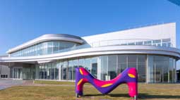
Meanwhile in other news, Merck is to invest EUR20 million to expand R&D and manufacturing capabilities at its site in Shizuoka, Japan. As part of this plan, new infrastructure will be built to advance and accelerate innovations in the electronic materials space. The investment is scheduled to be completed by January 2022.
“Shizuoka is one of our key technology hubs in Japan focused on advanced material developments for the semiconductor and display industries. With the booming digital economy and greater focus on devices, servers and equipment, we see an increase in collaboration activities with our customers and research partners to develop new innovations,” said Anand Nambiar, Head of Semiconductor Materials at Merck.
With its expanded capabilities, the Shizuoka site will focus on optimising new material discovery, device integration, application testing, sampling, quality control, and manufacturing for the semiconductor and display industries. To support the growing demand of the electronic materials market, next-generation materials, including semiconductor materials such as patterning materials, dielectrics, metal hard masks, Hybrid-SOD, novel EUV-Rinse solutions, and Directed Self-Assembly materials (DSA), as well as display materials such as dielectrics, photoresist materials and quantum dot pixel color converters (QDPCC), will be developed and manufactured.
The local Shizuoka team will work closely with Merck’s R&D centres in China, Korea, Taiwan, and the US to explore new solutions.
Digital adoption has been accelerated by Covid-19. The need for faster and more reliable data processing, storage and bandwidth is increasing the demand for semiconductor materials. To enable rapid advancements in device innovation and ensure speed to market, Merck is committed to investing in its capabilities globally and partnering with the industry. The company also plans to make significant investments in research and supply capabilities in order to meet the growing industry demand for integrated circuits.
As part of these investments, a new facility with a surface area of 6,000 sq m was completed in January. The two-storey building is one of the largest scale facilities in the western part of the Shizuoka prefecture in Kakegawa City, Japan. It offers office space for 230 employees.
Since its founding in 1984, the Shizuoka site has been a leading innovator in the development of patterning materials such as photoresists, vapor-deposited materials, core resists, BARC siloxanes, polysilazane thin-films and photoresists for displays, contributing significantly to the global Semiconductor Materials business of Merck.
Merck adds that it offers integrated solutions across multiple wafer process steps and dimensions to enable these developments. The company’s expertise extends beyond materials and includes delivery tools, equipment, containers, and services. Additionally, the integration of Versum Materials, Inc. and Intermolecular, Inc., coupled with processes and R&D capabilities, allows Merck to accelerate the development of innovations in the electronic materials space, it added.
Subscribe to Get the Latest Updates from IMA Please click here
©2021 Injection Moulding Asia. All rights reserved.
